Driving the Future of Photonic Integrated Circuits: An Interview with Luis Torrijos
By Yosimar Porras
Published November 20, 2025
iPronics develops advanced Optical Circuit Switches (OCS) based on silicon photonics to meet the extreme connectivity demands of modern AI and HPC clusters, delivering unprecedented integration density and pushing the limits of photonic performance. Since 2019, the company has led the commercialization of programmable photonic integrated circuits, leveraging proprietary SiPh IP and highly efficient building blocks to enable reconfigurable, high-bandwidth optical architectures. At its core, iPronics’ PIC team drives innovation in scalable, high-performance photonic systems that power the next generation of data-infrastructure networks.
Advancements in the simulation and optimization of SiPh building blocks have enabled the development of the first commercially available SiPh Optical Circuit Switch the iPronics ONE-32.
This interview with Dr.Luis Torrijos, head of the PIC design team, offers insight into the company’s strategic vision, the technical challenges it faces, and future developments in photonics, particularly for AI and data center applications.
Picture: Dr. Luis Torrijos, Photonics Manager at iPronics
Role and Vision at iPronics
Luis, can you start by telling us about your role at iPronics and how your team’s vision aligns with the company’s mission to advance PIC?
I lead the (PIC) design team at iPronics, where I oversee chip development and contribute to the strategic direction of innovation and the product roadmap. Our team specializes in designing proprietary photonic architectures and custom building blocks tailored for data center applications, enabling performance levels beyond what can be achieved with standard foundry Process Design Kits (PDKs). Aligned with the company’s vision, our goal is to expand the adoption of optical fabrics for AI infrastructure and data centers through the development of advanced silicon photonics optical circuit switches.
Increasing integration density is a key goal for iPronics. Why is this critical for the future of PICs, and how does your team approach this challenge?
Silicon photonics has experienced rapid growth in recent years, following a trajectory similar to electronics decades ago. Today, photonic chips integrate thousands of components within die areas of just a few square millimeters. Our primary objective is to remain at the forefront of this technology by developing state-of-the-art PICs that enable applications in datacom and beyond. Achieving this requires addressing several key challenges, including the miniaturization of integrated components, managing a massive number of electrical inputs and outputs, and—most critically—minimizing optical loss. To tackle these, we employ a variety of simulation tools that assist us in the design process and develop complex electrical driving systems and software layers to keep pace with technological advancements.
To develop state-of-the-art PIC designs, iPronics partners with tier-1 suppliers that provide the most innovative simulation tools. iPronics uses these tools extensively in its core development workflow — from optical layout to packaging and thermal simulations — enabling robust, full-stack design and validation of PICs that perform reliably despite fabrication variability. These resilient components are foundational for energy-efficient, low-latency future data center interconnects essential to AI workloads.
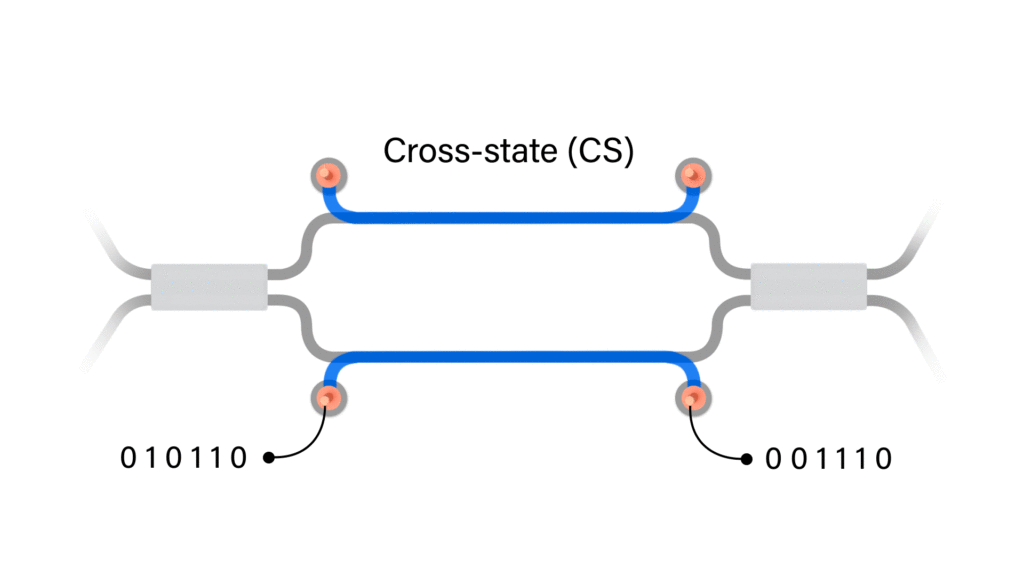
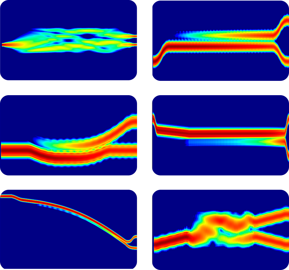
Figure 1. Artistic representation of a Programmable Unit Cell (PUC) of iPronics chip-level architecture showing the three different states bar, cross and tunable coupler. The device is a 2×2 Multimode Interferometer, controlled by a phase shifter in analogue operation. iPronics photonic layer for the ONE-32 consists of 2000 PUCs in a strictly non-blocking mesh arrangement. Some examples of light behavior simulation in different structures can be found in Figure 2.
Figure 2. Simulations of the light behavior in different 3dB splitter and combiner photonic building blocks. These images display numerical simulations of various design approaches used within the silicon photonics chip.
Reducing Losses in Photonic Circuits
Reducing losses in photonic circuits is a major challenge. How is iPronics addressing this, and what parallels can you draw with micro-electronics?
Optical loss can occur at multiple points within a PIC during light coupling, propagation through waveguides, or active tuning of the signal response, and it has a significant impact on link quality. To mitigate this, we apply advanced design methodologies throughout the entire PIC design process, from the creation of highly optimized building blocks to the development of complex photonic circuits and systems. This approach mirrors the evolution of electronics, where increasing system complexity drove the need to optimize each subsystem individually. In photonics, the situation is similar: the link budget in datacom applications is tightly constrained, requiring careful optimization of each circuit to maintain low overall loss. Achieving this depends on the strong synergy between the PIC architecture and the performance of the building blocks, ensuring the final chip, iPronics ONE-32 meets the required specifications.
The image shown in Figure 3 corresponds a wafer containing several ONE-32 chips utilized in our OCS product. It is based on a silicon photonics platform featuring over 100,000 integrated optical components, both passive and active, designed for full O-band operation to meet standard optical transceiver specifications in today’s datacenters, operating at speeds exceeding 100 Gbps.
Figure 3. Detail of a wafer showing several ONE-32 chips.
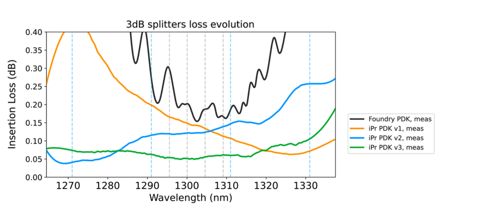
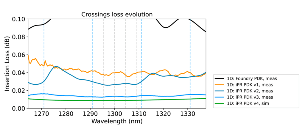
The main challenge in developing our ONE32 device has been optimizing the performance of its building blocks for datacenter applications. These applications require a flat spectral response across the entire O-band to ensure compatibility with DR, LWDM, and CWDM optics, while minimizing losses to reduce the need for high-gain amplification. Typical foundry PDKs building block performance (black line), is not enough to meet these standards so we developed our own designs., The performance of the diferent versions (v1, v2, v3) are shown in Figure 45 for 3dB splitters and for the crossing building blocks.
Figure 4. Representation of the evolution of the losses performance for our different versions of 3dB splitters (left) and crossings (right) in comparison with typical foundry PDK (black line)
Future of PICs and AI Applications
iPronics is known for its forward-thinking approach. What is your long-term vision for how PICs will evolve, particularly in terms of performance for AI applications?
Our vision is that photonics is here to complement electronics, not replace them. This synergy will be key to the successful deployment of technology in domains such as data centers and AI compute clusters. Photonics excels at transporting large volumes of data with minimal latency and low energy consumption. We see its future role as enabling high-performance interconnects between large computing clusters, where computation remains in the electrical domain, but data transport is handled optically. We believe silicon photonics is exceptionally well suited for developing (OCS), replacing traditional bulky mechanical systems with reliable solid-state chips.
Read more about this in his last publication: Link
Future Developments
What can you tell us about the future of iPronics’ optical switch and upcoming developments?
As mentioned earlier, we develop optical switches with silicon photonic chips at their core. This approach offers clear advantages over other solutions in terms of reconfiguration time, cost, and form factor. Another key aspect of our technology is that it achieves near-lossless operation by incorporating optical amplifiers to compensate for PIC losses. Looking ahead, we envision scaling the radix beyond a hundred ports while maintaining low loss and crosstalk, all within a tiny chip only a few square millimeters in size.
For readers less familiar with programmable silicon photonics, can you briefly explain what makes this technology unique?
Programmable silicon photonics allows for dynamic reconfiguration of optical circuits, enabling a single chip to perform multiple functions depending on the application. This flexibility is achieved through integrated tuning elements that modify the behavior of photonic components in real time. Such adaptability is crucial for modern data centers and AI systems, where workloads and connectivity requirements are constantly evolving.
At iPronics, we strongly believe that photonics will play a key role in enabling data centers to meet the demanding requirements of AI workloads. Optical Circuit Switches based on silicon photonics offer unmatched scalability, energy efficiency, and performance for next-generation infrastructures. Our commitment is to remain at the forefront of this technological evolution, driving innovation in programmable photonic architectures. We are proud and excited to lead this transformation.